Recently, the team of Professor Chen Peng and Zhang Rong from School of Electronic Science and Engineering published a research paper, titled "A Lateral AlGaN/GaN Schottky barrier diode with 0.36 V turn-on voltage and 10 kV breakdown voltage by using double barrier anode structure," on the Journal Chip. The research achieved a lateral AlGaN/GaN Schottky barrier diode with a 0.36 V turn-on voltage and a 10 kV breakdown voltage by employing a double barrier anode structure. Dr. Xu Ru is the first author, and the corresponding authors are Prof. Chen Peng, Prof. Zhang Rong, and Prof. Zheng Youdou. (https://doi.org/10.1016/j.chip.2023.100079)

III-V nitrides are typical wide-bandgap semiconductor materials. Among these, gallium nitride (GaN) is an excellent representative and finds extensive applications in the optoelectronics and power electronics fields. In particular, the AlGaN/GaN structure can generate a two-dimensional electron gas (2-DEG) with high electron concentration (~1×10¹³ cm⁻²) and high electron mobility (~2000 cm²/V·s). Combined with the high critical field (~3.3 MV/cm), power electronic devices based on AlGaN/GaN can have faster switching speeds, lower on-resistance, and higher breakdown voltages. They have a wide range of potential applications, including consumer electronics, automotive electronics, new energy, industrial motors, and even ultra-high voltage (UHV, >10 kV) electronic fields. Among these devices, power Schottky barrier diodes (SBDs) are particularly important and are one of the core components in power conversion systems. One of the key issues in developing GaN power SBDs is to create ultra-low loss/high-power devices, which involves effectively lowering the device's forward turn-on voltage (Von) and significantly increasing the breakdown voltage (BV) of the GaN SBD. Low Von / low specific on-resistance (Ron,sp) and high BV with low leakage current (Ileakage) are crucial for high-performance AlGaN/GaN power SBDs, especially for low loss and high-efficiency power transmission systems. In recent years, numerous high-performance AlGaN/GaN SBDs have been reported, with Von ranging from 0.2 V to 0.8 V and BV ranging from 0.13 kV to 10.0 kV. However, Von, Ileakage, and BV are mainly determined by the Schottky contacts, making it difficult to simultaneously improve all three parameters.
This research group has developed high-voltage GaN SBDs by studying the breakdown mechanism, leakage current transport mechanism, and depletion mechanism of GaN SBDs, focusing on reducing and optimizing the surface electric field during reverse bias of the device, anode trench preparation process, buffer layer and substrate material, and anode structure. Various terminal structures have been demonstrated to optimize the high-voltage SBD breakdown voltage, including our earlier reported 2.7-kV and 3.4-kV AlGaN/GaN SBDs with field plates²⁻³. According to the researcher’s previous studies, significant improvement in BV for AlGaN/GaN Schottky barrier diodes on Si substrates remains challenging. By using high-quality GaN material grown on sapphire substrates, they have reported high-performance AlGaN/GaN SBDs with BV exceeding 10 kV⁴⁻⁵.
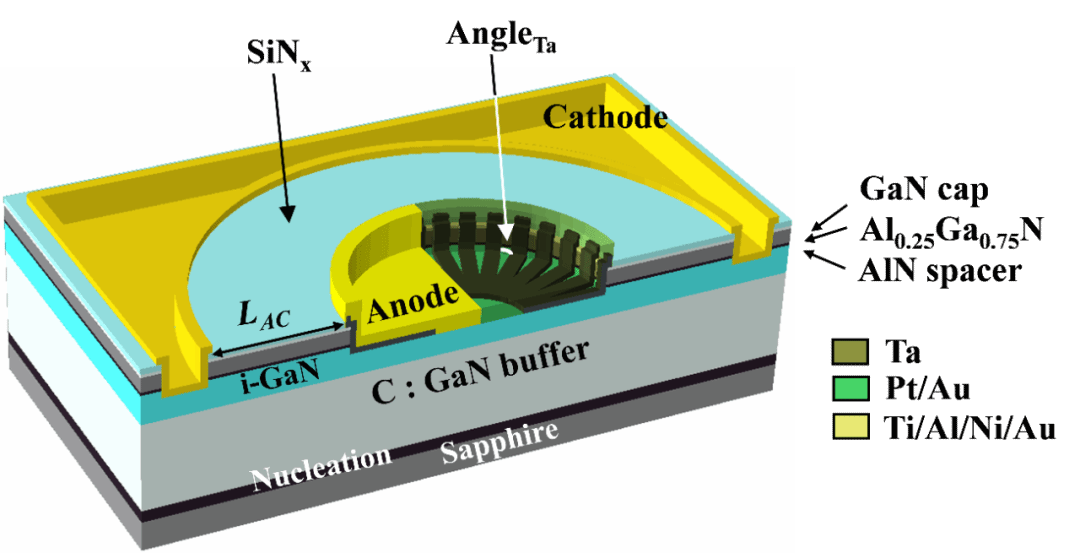
Fig. 1 | Schematic diagram of lateral AlGaN/GaN SBDs with serrated DBA structure on sapphire substrate.
To maintain high breakdown voltage of the Schottky electrode while using low work function metal, a new electrode structure design is required. In this work, we have designed and prepared a double barrier anode structure AlGaN/GaN SBD, based on analyzing the depletion mechanism of the Schottky barrier. Researcher proposed a double barrier anode (DBA) structure composed of high work function (platinum Pt, 5.65 eV) and low work function (tantalum Ta, 4.25 eV) metals⁶. The researcher innovatively combined the characteristics of these two metals and arranged them in an alternating serrated pattern, as shown in Fig. 1. The mechanism for reducing the device's forward voltage was studied using Silvaco software. The study found that the device's forward voltage during normal operation is mainly determined by the low work function metal Ta, while the leakage and breakdown during reverse operation are mainly determined by the metal Pt. This unique property is primarily determined by the relationship between the barrier height and depletion layer width of the Schottky structure. Thanks to the support of high-quality carbon-doped GaN buffer layers on sapphire substrates, the final sapphire substrate AlGaN/GaN SBD has a forward voltage of 0.36 V, effectively lowering the forward voltage compared to traditional Pt electrode structure devices by approximately 50%. To evaluate the consistency of device performance, we tested and analyzed 40 DBA SBDs, with an average Von of 0.37 V and a dominant value of 0.36 V, as shown in Fig. 2.

Fig. 2 | (a) Forward I-V characteristics of 40 DBA SBD devices, (b) Turn-on voltage distribution.
For the reverse I-V characteristics, the leakage current of the DBA anode device is slightly higher compared to the Pt anode, but it is lower by two orders of magnitude compared to the Ta anode device. Meanwhile, the breakdown voltage of the device is consistent with the Pt anode, both exceeding 10 kV, surpassing the 7 kV of the Ta anode device, as shown in Fig. 3. The characteristic specific on-resistance Ron,sp of the device is 25.1 mΩ·cm², the Ileakage is 2.5×10⁻⁶ A/mm, and the P-FOM is as high as 4.0 GW/cm².

Fig. 3 | Reverse I-V characteristics of DBA anode device, Pt anode device and Ta anode device.
This work not only demonstrates higher BV and power P-FOM in all lateral GaN SBDs on all substrates, but also achieves a low forward voltage of 0.36 V at same time. The comparison reference curve of the BV and Von of the GaN-based lateral SBDs in this work may be seen in Fig. 7 of the original paper¹. This work showcases the high-performance potential of GaN-based power electronic devices and their potential applications in low-loss and high-efficiency power transmission systems.
Reference
1. Xu, R. et al. A lateral AlGaN/GaN Schottky barrier diode with 0.36-V turnon voltage and 10-kV breakdown voltage by using double-barrier anode structure. Chip 3, 100079 (2024).
2. Xu, R. et.al, 2.7-kV AlGaN/GaN Schottky barrier diode on silicon substrate with recessed-anode structure. Solid State Electron. 175, 107953 (2021).
3. Xu, R. et.al, 3.4-kV AlGaN/GaN Schottky barrier diode on silicon substrate with engineered anode structure. IEEE Electron Device Lett. 42, 208-211 (2021).
4. Xu, R. et.al. High power Figure-of-Merit, 10.6-kV AlGaN/GaN lateral Schottky barrier diode with single channel and sub-100-μm anode-to-cathode spacing. Preprint at https://doi.org/10.48550/arXiv.2108.06679 (2021).
5. Xu, R. et al. High power Figure-of-Merit, 10.6-kV AlGaN/GaN lateral Schottky barrier diode with single channel and sub-100-μm anode-to-cathode spacing. Small 18, 2270199 (2022).
6. Xu, R. et.al. A lateral AlGaN/GaN Schottky barrier diode with 0.36 V turn-on voltage and 10 kV breakdown voltage by using double barrier anode structure. Preprint at https://doi.org/10.48550/arXiv.2206.07881 (2022).
Link to the papar:
https://www.sciencedirect.com/science/article/pii/S2709472323000424
Source: School of Electronic Science and Engineering
Correspondent: Chen Peng